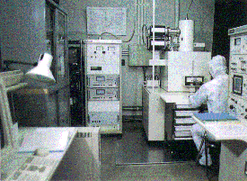
Facilities
This system has been specially designed and developed for fabrication of components for micro and integrated optics. The system employs analog/digital hybrid scanning scheme to enable efficient writing of analog patterns by extremely smooth linear/circular/curved scanning lines.
[2] Laser-beam writing system
We developed the laser-beam (LB) writing system for automatic patterning of channel waveguides in photoresist in order to fabricate LiNbO3 ICs beyond 30mm. The system consists of a closed-loop controlled X-Y translation stage driven by dc motors, a focusing optics of 0.442-mm He-Cd laser, and a LB intensity control circuit in synchronization with the stage. The patterning accuracy is < 0.2mm over the area of 10x10cm2 with the writing speed of typically 1.25mm/s. On the basis of our system, a practical LB writing system is now commercially available. Besides the waveguide patterning, the periodic LB dot writing technique was demonstrated recently for forming interdigital electrodes of the TE-TM mode conversion type of LiNbO3 wavelength filter, where the electrode period is controllable with an accuracy of the order of nanometer. The LB writing is also very promising for micro-machining in which a UV laser is used as the light source.
[3] ArF excimer laser ablation and CVD system:
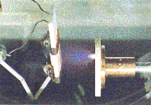 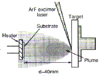 |
Waveguide fabrication based on photo-excited processes has been studied using 0.193-mm ArF excimer laser whose average power is 20W with the pulsewidth of 10 ns and the repetition rate of 10 to 100Hz. The recent interest is in deposition of LiNbO3 film on sapphire by ArF excimer laser ablation where a Li-rich LiNbO3 target is ablated to explode with a extremely high-temperature plasma (that is, plume), followed by deposition of single crystalline LiNbO3 film on c-cut sapphire. The resulting LiNbO3 film is well-oriented along the C-axis, and the propagation loss is reduced to 5dB/cm. The electrooptic coefficient r33 is also found to be 4.9pm/V which is nearly one sixth of that of bulk LiNbO3. Our effort is going on, directing at heteroepitaxial growth of LiNbO3 or LiTaO3 on Si which may lead to new types of hybrid optical ICs; for instance, an example is functional optical interconnects for electronic ICs on Si.
[4] Molecular beam epitaxy system

We have small MBE system consisting of a growth chamber with an ion pump and an introduction chamber for fabricating GaAs/AlGaAs waveguides on GaAs substrates.